Sensitivity Measurements
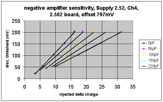
Sensitivity curves for a single channel (chan 4) of the positive and negative negative amplifier for different capacitances. The discriminator 'saturates' at about 300mV, i.e. with the starndard offset of 800mV we cannot use a threshold of more that 1.1V


Straight line fits to the above plot. The final sensitivity of the negative channel is around 14-15mV/fC at 0pF and 7-8mV/fC at 220pF.

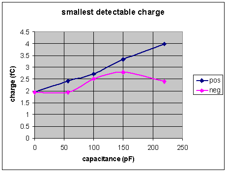
The following plot shows the extrapolated smallest detectable charge versus capacitance. The actual smallest detectable charge is smallest since the sensitivity curves 'bend' at small charges. The plot has to be improved with more statistics ....the extrapolation has of course quite a large error.
Sensitivity Variations
The sensitivities were measured on 10 positve boards (20 chips, 160channels) and 7 negative boards (14 chips, 112 channels).
Positive Amplifier


The channel to channel variations are smaller that the chip to chip variations. The reason for that has to be investigated. The reason for that must be something that is common to all channels, like biasing network, resistors on the board or even the supply voltage.


The 'positive no package' chips show a sensitivity of 15.93mV/fC with an r.m.s of 0.56mV/fC i.e. 3.54%.
The 'positive package' chips show a sensitivity of 14.5mV/fC with and r.m.s. of 0.62mV/fC i.e. 4.31%.
Subtracting the average sensitivity of each chip we find the following histograms:

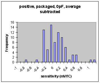
For the 'positive no package' chips we find an r.m.s of sqrt(8/7)*0.32mV/fC = 0.34mV/fC i.e. 2.15%.
For the 'positive package' chips we find an r.m.s of sqrt(8/7)*0.32mV/fC =0.34 i.e. 2.36%.
Negative Amplifier


As for the positive amplifier the channel to channel variations are smaller that the chip-chip variations.
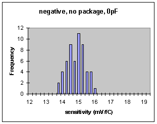
The 'negative no package' chips show a sensitivity of 14.73mV/fC with an r.m.s of 0.56mV/fC i.e. 3.8%.
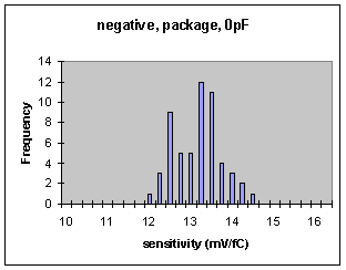
The 'negative package' chips show a sensitivity of 13.05mV/fC with and r.m.s. of 0.56mV/fC i.e. 4.3%.
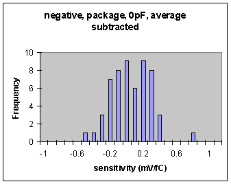
Subtracting the average sensitivity of each chip we find the following histograms:
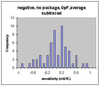
For the 'negative no package' chips we find an r.m.s of sqrt(8/7)*0.37mV/fC = 0.40mV/fC i.e. 2.7%.
For the 'negative package' chips we find an r.m.s of sqrt(8/7)*0.24mV/fC = 0.26mV/fC = i.e. 2.0%.
Minumum Detectable Charge
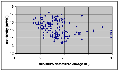
The extrapolated minimum detectable charge (or minimum threshold in fC) was measured by finding the intercept of the sensitivity curve with the 'fC' axis. The true minimum detectable charge is smaller then the extrapolated value since the sensitivity curver become nonlinear at small charges.
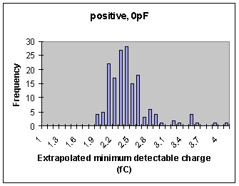
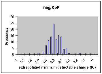
The average is at 2.4 fC with an r.m.s. of 0.37 fC for the positive chip and
an average of 2.4fC with an r.m.s. of 0.24fC for the negative chip.
The minimum detectable charge is defined by the discriminator which 'needs a certain minimum voltage pulse' in order to 'fire'. This is also shown by the fact that this charge is correlated with the sensitivity.
